500W Tabletop Class E
This transmitter is a PDM (pulse duration) modulated Class E AM transmitter for 80 and 160m that uses 12 x FQA11N90 FET's in the output. It easily produces 500W carrier output.
The transmitter includes a single chip DDS RF exciter.
All metering, relay sequencing and DDS programming is performed by a Parallax Stamp microcontroller and LCD display.
A big part of this project was the metalwork which took me several weeks to fabricate. I started with a surplus commercial enclosure and beefed it up to improve both its strength and RF shielding.
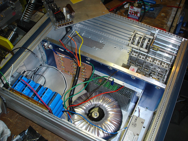
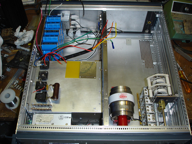
An 1/8" aluminum plate separates the left and right half of the enclosure. The PDM modulator, DDS generator and power supply are built into the left half and the Power amplifier and tank circuit in the right half.

The toroidal power transformer is rated 1KVA - overkill for this transmitter. It is a medical grade isolation transformer that has 2 x 120V pri and 2 x 0-100-120V sec. The price was right at $40 on Ebay! The two primaries are operated in series for low power operation and parallel for high power (from a 120V source). I used a similar 2KVA transformer in my big 20 FET Class E transmitter with excellent results.
The switching power supply module next to the toroidal transformer powers the PA drivers and several relays, it is rated 12V @ 4.2A.
In the RF section you can see a 1000pF vacuum variable (Tune), a 2500pF air variable (load) and a dual gang RF switch that will switch the tank coil and additional loading caps for 160m. Not visible is an additional small ganged switch which informs the micro-controller of the selected band. The heatsink is visible at the rear with about 70% of its surface area allocated to the RF section and 30% to the modulator. A small fan cools the heatsink - it is supported on rubber mounts and is barely audible when running.
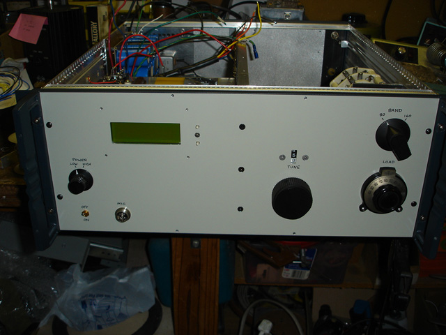
The front panel is clean and functional - on the left you see the the hi/lo power switch, main on/off power switch, mic connector and LCD display. To the right of the LCD display are 2 small push buttons that tune the DDS up or down in frequency. On the right are the tank tune and load controls and the band switch. The LCD display shows the recommended tune and load settings for the selected frequency when in receive or standby mode (facilitating a quick tuneup when changing frequencies).
Below is a picture of the DDS exciter. This small board provides 2 bi-phase outputs that drive 3 ea IXDD414 drivers that are mounted adjacent to each side of the PA (each IXDD414 drives 2 x FQA11N90 output FET's). The DDS chip is an Analog Devices AD9834. Performance is excellent with DDS spurs better than 70dB down.
The single POT on the board simultaneously adjusts the duty cycle of the 2 outputs. The duty cycle adjustment corrects for skew in the IXDD414's. I have found that approximately 40% on and 60% off works best. Power and programming connections are fed via the feedthru caps on the left and come from the microcontroller board.
This DDS is capable of tuning in very small frequency steps but I have chosen to limit it to 1KHz steps in software to simplify tuning. 1KHz resolution is adequate for AM work.

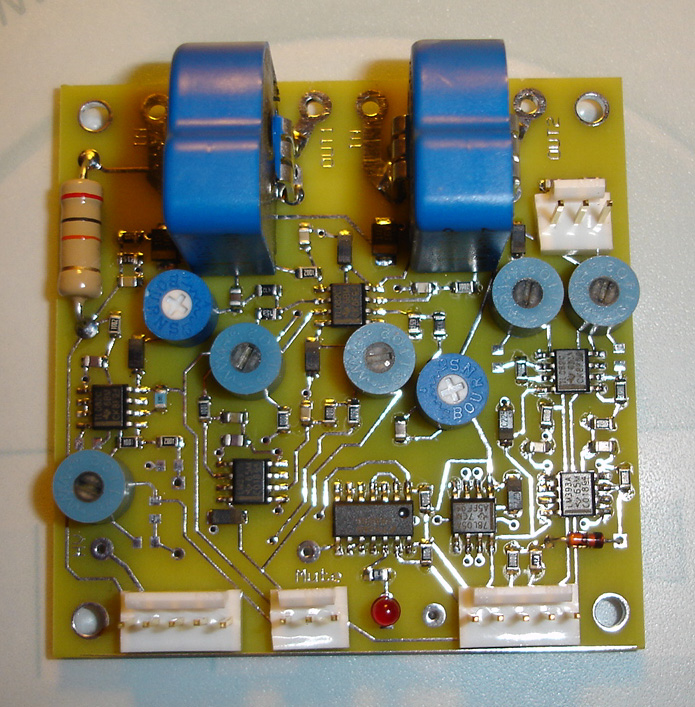
The board below is the PA current sense board; hall effect current sensors (large blue parts) are used to measure the current to each leg of the PA.
This board scales the measured current and voltages and feeds them to the ADC on the micro-controller board. Additional inputs are also provided to measure and display output power. Over-current protection circuitry on this board reacts very quickly to such a condition and disables the PDM pulse train (HV supply to PA).
The large resistor on the left scales the PDM output voltage (the PDM input voltage sample is fed to this board from an external resistive divider).
4 of the pots trim and scale the outputs from the hall sensors, 2 scale the forward and reflected power inputs and one sets the overcurrent trip point.
The micro-controller board (below) is built up on perfboard. It uses a Parallax BS2SX Stamp module that is very easy to program in Basic! The chip above it is an 8channel 10 bit ADC. This board is the heart of the transmitter and controls all relay sequencing, programs the DDS, computes and displays input power etc.

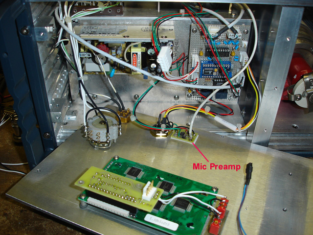
In the pic below you can see the micro-controller board mounted inside the transmitter and to the left of it a small power supply module which provides +5,-12 and +12 to the low level circuits. Supplies like these are very inexpensive nowadays and simplify construction.
On the front panel (facing down), you can see the LCD dislay module (a standard 4 x 20) and a small piggy back board attached to it that serializes the interface to the LCD module (minimizing I/O connections to the microcontroller).
You can also see the mic preamp; a small SMT board located adjacent to the mic input connector. Amplifying the audio input directly at the mic connection minimizes the opportunity for ground loops and hum .You may notice several wires going to the mic connector; this is because it is also used as the programming port to update the micro-controller firmware!
The PDM generator and input filter was built deadbug style on a piece of copper clad FR4 (see below). It is mounted directly above the main HV toroidal transformer together with the current sense/protection board, HV bridge rectifiers (top left) and power relays (lower left). The PDM modulator IC I used is a UCC25702 which will run happily from a +12V supply.
The 25W resistor (brown) and relays to the left of it are the HV soft start and on/off circuit.

Despite the audio circuits being mounted close to the HV transformer there is absolutely no sign of any hum in the audio. The audio circuits are very compact, minimizing the opportunity for induced AC hum. I also paid special attention to grounding. In fact the only detrimental effect due to proximity to the HV transformer that I have detected so far is a small induced component on the Hall effect sensors - however, it is sufficiently small not to affect operation.
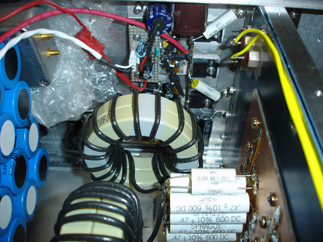
Below you can see the PDM modulator and output filter. The modulator uses 3 x IRFP260N's operated in parallel that are driven by an IXDD414 which is in turn driven by an opto-isolator. The PDM filter is a simple Butterworth design that uses 2 x CH777060 stacked cores for each inductor. These cores are supported by acylic blocks screwed to the base plate. The 2 yellow wires visible in the pic below feed modulated HV from the output of the PDM filter (via the hall effect current sensors) through the central wall (feedthru caps) to the PA circuits.
The copper circuit board on the right of the pic below has copper buss bars soldered across it and acts as the central grounding point for the HV power supply and modulator. It is bolted to the plate that runs down the center of the transmitter that is in turn bolted to the common heatsink at the rear (all using many screws). The common heatsink supports both the PDM modulator and RF PA circuits. In this way all high current ground paths are very tightly bonded.
The modulator was first tested with high power resistors to simulate the load presented by the RF PA circuits and found to work very well.
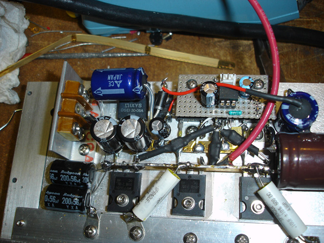

In the pic above you can also see the DDS generator squeezed in behind the capacitor bank. That ended up being its final home. 2 short coax cables feed the the drivers in the PA section.
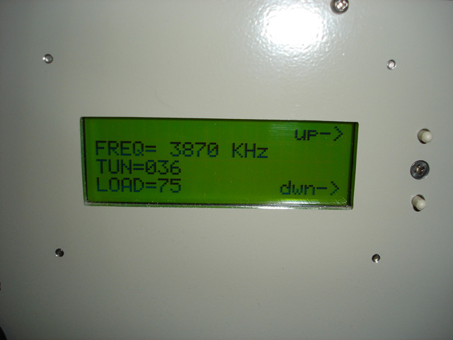
The pics below show the front panel display:
In receive mode (below) the frequency can be tuned using the up and down tune buttons. The recommended Tune and Load positions for the selected frequency are also displayed to facilitate tune up.
In transmit mode (below), current to each half of the PA (Id1 and Id2), PDM input voltage (Vin) and PDM output voltage (Vrf) are displayed. Input power is computed by (Id1+Id2)*Vrf and also displayed. The transmit frequency is also displayed but can not be changed while transmitting.
This picture was taken when the modulator was loaded with resistors. The mismatch in currents (Id1 vs. ID2) is because I had different value resistors in each leg.

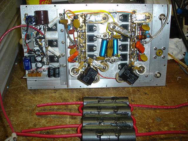
The picture below shows my initial design PA and modulator sections assembled on the heatsink. The output transformers (2 of them glued together) are also shown.
I later removed some of the doorknob shunt capacitors and rewound the output transformers using a coaxial approach (see pics later).
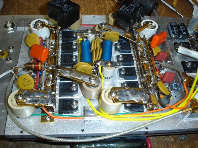
Here's a closer view of the RF section. Pic shows 3 x 500pF shunt caps (doorknobs) + an additional 1000pF cap switched in by a relay, per section.
The IXDD414 drivers (6 of them) share a common 12V power rail (from a commercial switching brick) which is very well decoupled. In the center you can see the decoupling caps for the HV feed (2 x 0.1uF poly and 5 x .01 cer disc per FET string).
The 1.3K 2W carbon resistor is part of a voltage divider that monitors the drain waveform of one section (feeds a BNC connector on the rear panel).
2 coax cables with SMB connectors feed the drive signal from the DDS generator through the center dividing wall.
Here it is installed in the chassis with the new output transformers soldered in place. Note that I ended up removing 4 of the doorknob capacitors - this improved the efficiency and raised the peak drain voltage to about 3.5 x Vdd).

The output transformers are wound using a coaxial method for optimum coupling. The primary is a heavy braid through which the secondary (#8awg) is threaded.

The tank coil uses 1/4" copper tubing for the 80m section and 3/16" for the 160m extension. 3" ID.
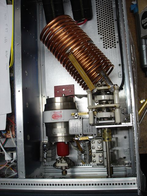
I originally used 2 x 500pF doorknob caps to pad the loading capacitor but found these got very warm and were hurting efficiency. I ended up using a bunch of 100pF mica caps in parallel (I found a big bag of these at a local ham swap). I have 10 x 100pF (=1000pF) of fixed capacitance in parallel with the variable loading capacitor and I also switch in an additional 400pF when on 160m. The multi-section adjustable capacitor has 2 ground wipers per section (10 all together) and appears able to handle significant RF current.

The band switch is a high current RF switch. Do not try to use a skimpy switch here - it will burn up due to the high RF current (I know from experience).
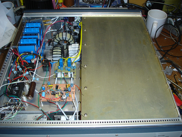
A lid is fitted to the RF section to keep things RF tight. There is also a lid that covers the entire unit (not shown).
When I first started testing this transmitter the efficiency was lower than expected; 81% on 80m and 87% on 160m. Accurate efficiency numbers require accurate power measurement - I'm measuring the output power using a 350MHZ oscilloscope to measure the pk-pk voltage across my 50 ohm dummy load (200V pk-pk = 100W and 400Vpk-pk = 400W). This seems to be the most accurate method I can think of. Input power is accurately computed and displayed on the front panel LCD.
After a lot of experimentation I was able to increase the efficiency to 90% on 80m and about 92% on 160m! This was accomplished by removing 2 of the 3 drain shunt caps that I had initially installed on each half of the PA, changing the output transformers to coaxial, using fixed mica loading caps and changing the 80m tank coil to 1/4" tubing.
At 400W output power the input power is now 444W on 80m. This means 44W is being dissipated as heat. I estimate about 15W of this is being dissipated in the output transformers (which can get quite warm), about 8W in the tank coil and the rest (~ 20W) I think is being dissipated by the FET's (into the heatsink).
This transmitter is very nearly finished now and has already been on the air with excellent audio reports.
Shortly after completion I managed to blow up the PA!
This prompted me to make a few changes. Below is a pic of the final PA arrangement.

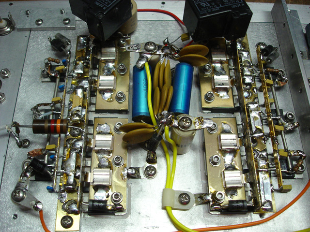
I changed the shunt caps to 220pF mica caps. These are soldered to brass plates above the PA transistors. The brass plates are grounded through the transistor mounting screws and also to a ground tab. This gives 880pF per side. I had only 5oopF and 200pF on each side before (this balanced the PA current). Efficiency was ~ 90% on 80m, now it is only about 87% but the peak drain voltage is a little lower.
I skimped on tranzorbs the first time around - BIG mistake! They are installed now.
Since I run all of my drivers from a common switching power supply, I added series diodes in each leg to isolate them.
Finally I spent some time optimizing the over-current protection. The idea is to dynamically adjust the trip point with the modulating signal. The problem was that the bandwidth out of the hall sensors was less than the sampled drain voltage (modulated) causing me to miss-adjust the trip point (to avoid tripping on sharp audio transients). By balancing the bandwidths of the two paths into the trip comparators the protection circuit works much better.

In the above pic you can see my PA and drivers on the left and the PDM modular on the right - both share a common heatsink. I found that a small fan was required to keep the heatsink cool (turns on when transmitting and is very quiet (not much air required).